

Digital Integrated circuits are produced using different circuit configurations and production Technologies. Each approach of digital integrated circuits is called the Logic family. A logic family is a collection of different integrated circuit chips with similar input,output and internal circuit characteristics, different logic gate functions. These logic families vary by speed, power consumption, cost, voltage levels.
The digital Integrated circuits are designed using bipolar devices or metal Oxide Semiconductor or combination of both. Mostly the Logic families are falls under the first kind Bipolar logic family and the Unipolar logic family.
Bipolar Logic Family
Saturated Bipolar Logic Families
Diode Logic
Resistor Transistor Logic
Diode Transistor Logic
Integrated Injection Logic
Transistor Transistor Logic
High Threshold Logic
Non-Saturated Bipolar Logic Families
Schottky TTL
Emitter Coupled Logic(ECL)
Unipolar Logic Family
Unipolar Logic families consist of Metal Oxide Semiconductor Logic families
P-type MOS Logic
N-type MOS(NMOS) logic
Complementary MOS(CMOS) logic
Bipolar MOS(BiMOS) logic
Bipolar CMOS(BiCMOS) logic
- Diode Logic
- Resistor Transistor Logic
- Diode Transistor Logic
- Integrated Injection Logic
- Transistor Transistor Logic
- Schottky TTL
- CMOS
- BiCMOS
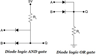
Diode Logic
This Diode logic functions as switch circuit. Here in this Diode logic family only resistor and diode will be used. The resistor will be used as either series with diode or parallel.
The Advantage of Diode logic family is simplicity of the circuit. We can implement only OR and AND gate by using the Diode logic family.
In most cases the Diode Logic family used as switch circuit. When diode in forward bias it works as closed switch, when it is in reversed bias it works as open switch.
Resistor Transistor Logic
Resistor Transistor Logic families are Saturated Bipolar Transistor. It made of with resistor along with Transistor. The resistor is connected in the input terminals of the logic circuit and the transistor at it’s output side. Transistors emitter terminals are connected to the to the ground and the collector terminals of the Transistor tight together and connected resistor along with the supply voltage terminal. And the input is given along with the resistor and the resistor is connected along with the base terminal of Transistor.
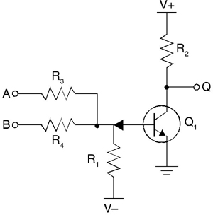
Pic: RTL NOR gate
Advantage
It is simplicity, minimum transistors are required to implement logic expression and it is much improved logic families than diode-transistor logic and transistor-transistor logic
Disadvantage
It has high power dissipation specially at when transistor at logic 1.
Diode Transistor Logic(DTL)
Diode Transistor logic family is a Saturated Bipolar Transistor Logic which consist of diode at the input Terminal and the Transistor at the output terminal.
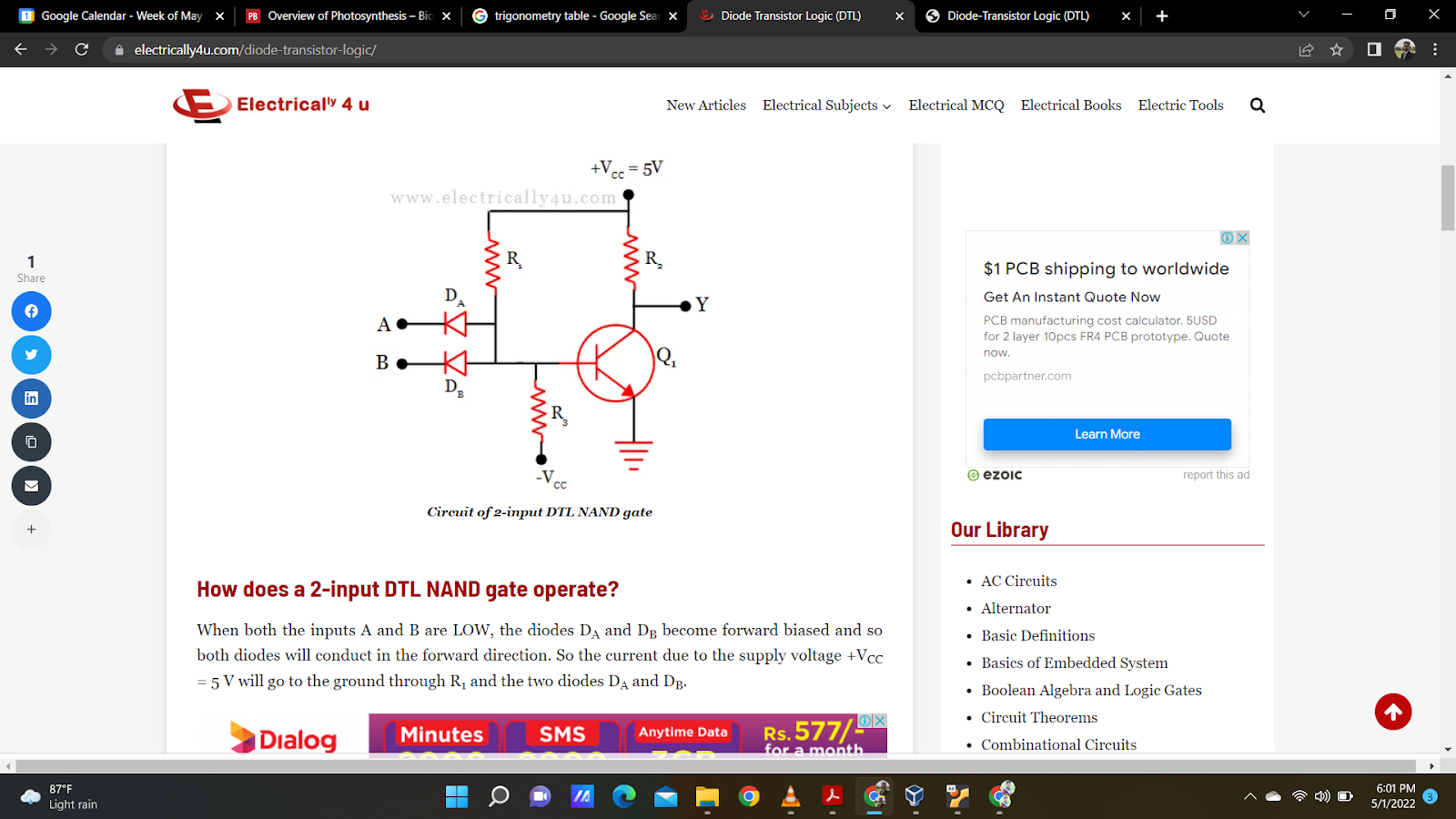
Pic from www.electrically4u.com
The above figure shows that 2 input DTL NAND gate logic. Here the diode Da,Db,R1 resistors are the input. The output are the common emitter configuration transistor Q1 and the resistor R2.
When two of the input Terminals A and B are LOW then the diode will be in the Forward bias.the supply voltage will flow through the resistor r1 and through the diode Da and Db. The voltage does not sufficient flow through the transistor so it will remain same as cut off stage. The output at y will only be HIGH.
When either A or B is HIGH the current will flow through the the diode which is having LOW at it’s input terminal the transistor will remain in the cut off region. The output terminal Y will also be at logic 1.
When both the inputs A and B are HIGH, which will reverse bias both the diode. Then the voltage from supply vcc will be enough to conduct current through transistor from collector to emitter terminal. Here the voltage gets dropped in the resistor r2. The output voltage at y is 0v which means LOW logic.
It is better advantage than using RTL logic. It has improved Noise margin, Fan-out. However the propagation delay is more for this device, when compared to Transistor Transistor Logic but it is faster than RTL.
Integrated injection Logic
Integrated injection logic family is a saturated bipolar logic family. Which is made of multiple collector bipolar junction transistors. It has speed more comparable to Transistor Transistor logic and low power than CMOS. The gates can be made smaller with this logic family than CMOS because no complementary transistors are not needed. And logic levels of it are very close HIGH:0.7V LOW:0.2V.

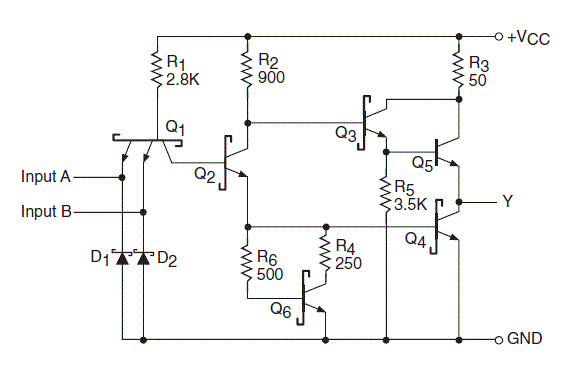
Transistor Transistor Logic family
It’s a bipolar saturated type transistor transistor logic family. It’s a logic family made up of BJTs . This family of transistor made up of with several resistor and BJTs. it has several inputs.
Types of Transistor-Transistor Logic
Standard TTL
Fast TTL
Schottky TTL
High Power TTL
Low Power TTL
Advance Schottky TTL
TTL Family Features
Logic Low is at 0v or 0.2v
Logic High level is at 5v.
Typical fan out is 10.It means it support at most 10 gates at its output.
The basic TTL device draws a power of 10mW. Which reduces the use of schottky devices.
The average noise margin is about 0.4v
Propagation delay is about 9ns.
The basic gate used in TTL is NAND. It has strong Noise Immunity. And the clock rate is 35MHz
Advantage and disadvantage of TTL circuit
The main benefit of TTL logic is we can easily interface with other circuits and the ability to produce different logic function because it has good noise margin.
It has good fan-in. Which means the i/p signals that can be accepted through an input.
The main drawback of TTL is high current utilization. It can lead to offensive functioning because o/p states will be turned off.
When the arrival of CMOS TTL is replaced but it quietly used in robust applications& logic gates fairly cheap.
TTL Applications
Used controller application for providing 0 to 5v
Used in switching devices in driving lamps and relays
Used in processors of mini computer
Used in printers and video display terminals.
Schottky TTL
This is included in non-saturated bipolar Logic Families . It’s design was used to speed up the process of Operation. It has fast operation than high power TTL. The power dissipation for both the TTL are same. The schottky further divided into many parts like Low power schottky,advanced low power schottky and advance schottky.
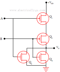
CMOS logic Family
It’s a Unipolar Logic Family. Complementary logic devices uses both N-channel and P-channel MOSFET devices. CMOS has greater complexity circuits than PMOS and NMOS circuits. But it has speed operation and less power dissipation. and CMOS has more fan-out and better noise margin. Noise margin include operation environment,electricity and magnetism field , radiation,power supply. Some transistor switching operation will also have unwanted noise. To ensure that the transistor works under the specified noise condition, circuits must be designed with specified noice margins.
CMOS has NAND gate ,NOR gate and so on.
NAND gate as follows
Bipolar CMOS(BiCMOS)Logic
It is one of the major technology and is highly developed technology by the combination of bipolar Junction Transistor and CMOS transistor. It is very complex technology with PMOS and NMOS amalgamated each other with each other with lower power consumption cause of bipolar transistor and having high speed cause of CMOS technology. MOSFET grands high input impedance and logic gates and bipolar transistor provides high current gain.
It’s Technology is well suited for input output intensive applications,it can be used in applications such as adders,ADC,DAC and mixer.
Advantage of Bicmos Technology,
Analog amplifier design is facilitated and improved by using high input impedance CMOS circuit as input and remaining are realized by using bipolar transistor.
High load current sinking and sourcing can be provided by BiCMOS devices as per requirements.
It has low power dissipation than bipolar technology alone.
This circuit frequently use in analog power managing and amplifier circuit.
It offers input/output intensive application and ,it has flexible input/output.
It has improved speed performance than CMOS.
Drawback of BiCMOS technology
The fabrication technology for this family comprised of CMOS and Bipolar so it has complexity.
Due to the complexity, it’s price also high


سئو در کرج با کمک سئوکار کرج می تواند تاثیر بسزایی در رشد کسب و کارهای داخلی داشته باشد. یک متخصص سئو با تجزیه و تحلیل دقیق کلمات کلیدی، بهینه سازی ساختار سایت و تولید محتوای هدفمند به بهبود رتبه سایت در نتایج جستجوی گوگل کمک می کند. این فرآیند باعث افزایش ترافیک ارگانیک و جذب مشتریان جدید می شود که در نهایت منجر به رشد فروش و تقویت برند می شود.
ReplyDeleteAlways surprises me with new items. buy a vending machine
ReplyDelete